
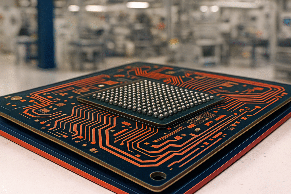
Semiconductor Package Design
Semiconductor Package Design is the work of placing a tiny chip into a protective “home” so it can connect to the outside world and run cool, fast, and reliably. We choose the right package style (like QFN, BGA, or wafer-level), design the tiny wiring and layers inside, and check heat, power, and signal quality so nothing fails later. The goal is simple: a package that’s easy to make, fits your board, meets performance targets, and lasts in the field.
Flip-Chip & BGA Packages
We design flip-chip and BGA packages optimized for signal integrity, power delivery, and warpage control. Deliverables include bump maps, escape routing, substrate stack-ups, and SI/PI/thermal models. We tune layer counts and via strategies to balance cost and performance, validate with simulations, and release JEDEC-compliant drawings and Gerbers ready for OSAT build.
High-I/O, low-inductance packaging for performance silicon

QFN / LGA Wire-Bond Packages
From small-outline QFNs to large LGA, we engineer leadframe and pad layouts, bond-finger optimization, and pad ring strategies for yield and reliability. Designs include thermal pad sizing, mold and singulation rules, and MSL planning. We provide assembly design rules and qualification plans aligned with J-STD-020 and JESD47.
Cost-optimized, robust packages for volume products
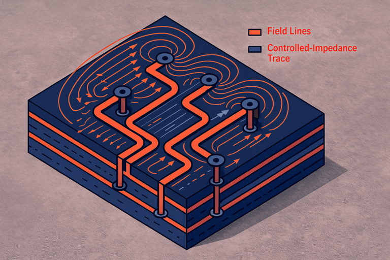
Substrate & Signal/Power Integrity Co-Design
We co-design die I/O maps and substrate routing to meet impedance, crosstalk, and PDN impedance goals. Outputs include controlled-impedance traces, return-path planning, decap placement, and S-parameter/IBIS models for system teams. Early extraction shortens board bring-up and reduces spins
Stack-up, impedance, and PDN targets—engineered together

Thermal & Reliability Engineering
We size lids, heat spreaders, and TIMs to hit θJA/θJC targets, run CFD and compact model creation, and assess CTE-driven warpage and stress. Reliability plans cover HTOL, TCT, drop/vibration, and moisture sensitivity. Results are packaged as thermal models and qualification reports for production release.