Die Scope Analysis ( Semiconductor Die Cross Section )
Understanding IC Structure from Silicon to System-Level Integration
Semiconductor devices are the backbone of modern electronics. From smartphones to industrial systems, every product depends on how efficiently a chip is designed and packaged. At Saktech, we provide deep expertise in semiconductor die cross section analysis and packaging evaluation, enabling better performance, reliability, and cost optimization.
What is a Semiconductor Die Cross Section?
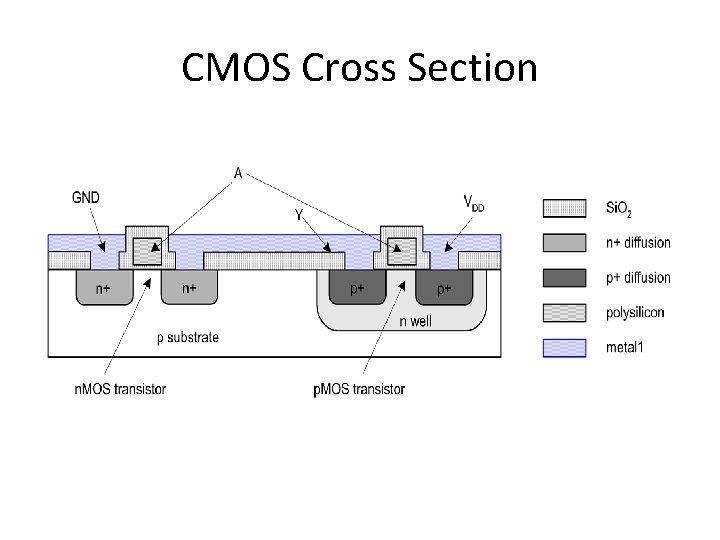
A semiconductor die cross section reveals the internal architecture of an integrated circuit (IC). It shows how transistors, interconnects, and insulating layers are stacked on a silicon substrate.
Key Layers in a Die Structure
Silicon Substrate – The base material where the chip is built
Doped Regions (N-type / P-type) – Form transistors for switching
Gate Structure – Controls electrical flow in transistors
Isolation Layers (STI) – Prevent leakage between components
Interlayer Dielectric (ILD) – Insulates metal layers
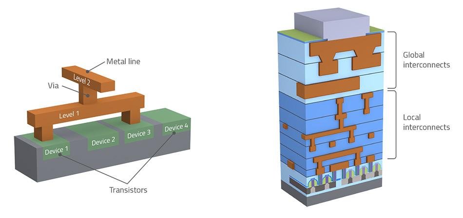
Metal Interconnects (M1–Mn) – Connect billions of transistors
Passivation Layer – Protects the chip from environmental damage
This layered architecture enables high-density, high-speed electronic functionality in modern ICs.
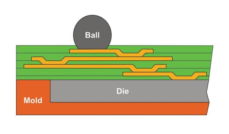
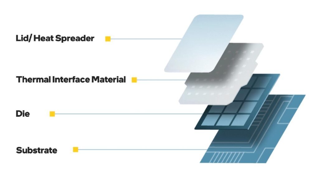
Semiconductor Packaging (Outside the Chip)
Core elements:
Die attach
Substrate / leadframe
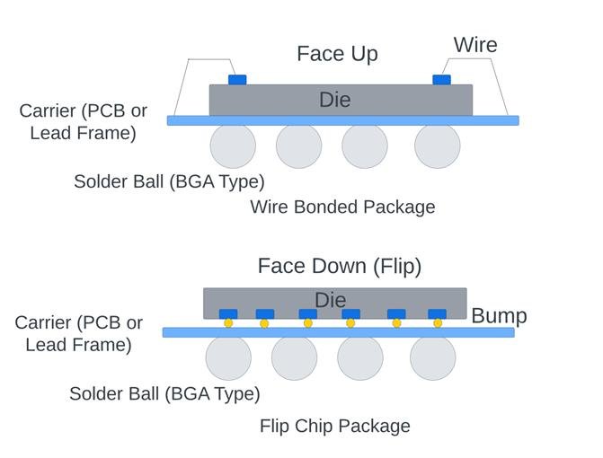
Interconnection (wire bond or flip-chip)
Mold compound (protection)
External pins / balls
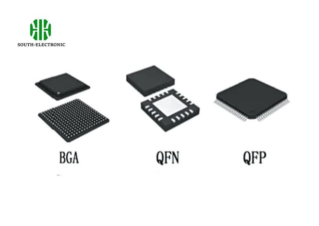
Key Packaging Types
QFN / DFN – compact, cost-effective
QFP – leaded package
BGA – high performance
WLCSP / 3D IC – advanced packaging
Analysis Focus (Engineering & Sourcing)
Die size → impacts cost & yield
Package type → QFN (low cost) vs BGA (high performance)
Interconnect → wire bond vs flip-chip
Thermal design → heat dissipation capability
Pin count & substrate → complexity and cost
Die structure defines how a chip functions, while packaging determines how it performs in real-world applications. Optimizing both ensures better performance, reliability, and cost efficiency.